
Artificial intelligence/Machine Learning-driven modeling reduces time-to-market for faster Design Technology Co-Optimization development and accelerates model parameter extraction for advanced nodes, RF, and power applications
Keysight Technologies, Inc. (NYSE: KEYS) today announced the release of the new Machine Learning Toolkit in the latest Keysight Device Modeling Software Suite. This new solution reduces model development and extraction time from weeks to hours, enabling faster Process Design Kit (PDK) delivery and Design Technology Co-Optimization (DTCO) applications.
This press release features multimedia. View the full release here: https://www.businesswire.com/news/home/20260115914104/en/
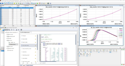
Machine Learning Toolkit speeds up model development time from weeks to hours.
The semiconductor industry is undergoing rapid transformation, driven by advanced architectures such as gate-all-around (GAA) transistors, wide-bandgap materials such as GaN and SiC, and heterogeneous integration strategies including chiplets and 3D stacking. While these innovations drive performance, they also create complex modeling and parameter extraction challenges. Traditional workflows rely on physics-based compact models and manual parameter extraction, forcing engineers to adjust hundreds of interconnected parameters across multiple operating conditions, a process that can take weeks and often struggles to achieve optimal results. With increasingly tight schedules, faster, more predictive, and automated artificial intelligence/Machine Learning (AI/ML)-driven modeling solutions are now essential.
Keysight’s new Machine Learning Toolkit, featuring an ML optimizer, auto-extraction flows, and utilities within Device Modeling MBP 2026, tackles these challenges by introducing a framework that combines advanced neural network architectures with ML-based optimization. Using this toolkit, auto-extraction can reduce the parameter extraction steps from over 200 to fewer than 10, accelerating PDK delivery, automating DTCO, and speeding up time-to-market.
Key Features and Benefits:
- Accelerated Parameter Extraction: Reduces hundreds of manual steps to 5 to 6 automated steps, enabling global optimization of 80+ parameters in a single run, capturing secondary effects, temperature variations, and dynamic behaviors. This solution eliminates repetitive manual tuning and improves predictive accuracy across DC, RF, and large-signal domains.
- Automated Workflow: Integrates seamlessly with Keysight’s Device Modeling platform, supporting Python-based customization and robust automated modeling flow.
- Scalable Across Technologies: Workflows adapt easily to FinFET, GAA, GaN, SiC, and bipolar devices, ensuring repeatable and reusable flows for multiple process nodes.
- Improved DTCO Efficiency: Enables faster feedback loops between device and circuit design, reducing PDK development cycles from weeks to days.
Nilesh Kamdar, General Manager of Keysight EDA, said: “AI/ML is fundamentally transforming the traditional workflows and methodologies of compact modeling. With the new Machine Learning Toolkit, we empower our customers to deliver more predictive, higher-quality models in significantly less time — accelerating PDK development and helping them keep pace with rapidly evolving semiconductor technologies.”
By leveraging AI/ML-driven modeling, Keysight enables semiconductor companies to accelerate innovation, reduce development risk, and maintain a competitive edge in a rapidly evolving market. For more details, visit Keysight Device Modeling Solutions.
Additional enhancements across other Keysight device modeling solutions include:
- Device Modeling MQA 2026: Introduced new rules related to the Aging Model QA for OMI and MOSRA.
- Device Modeling WaferPro 2025: Introduced a new remote-control feature for remote low-frequency noise testing with A-LFNA for enhanced flexibility and efficiency.
- A-LFNA 2026: Introduced new low-frequency noise stress test capability for seamless measurement from stress test to noise test.
Resources
- Video: Simplifying and Automating Compact Model Process with Machine-Learning
- White Paper: Accelerating Semiconductor Innovation through Machine Learning Driven Modeling
- Application Note: Accelerating Compact Model Parameter Extraction with the Machine Learning Optimizer
- Blog: From Equations to Intelligence: Integrating a Machine Learning Optimizer into Compact Model Extraction
About Keysight Technologies
At Keysight (NYSE: KEYS), we inspire and empower innovators to bring world-changing technologies to life. As an S&P 500 company, we’re delivering market-leading design, emulation, and test solutions to help engineers develop and deploy faster, with less risk, throughout the entire product life cycle. We’re a global innovation partner enabling customers in communications, industrial automation, aerospace and defense, automotive, semiconductor, and general electronics markets to accelerate innovation to connect and secure the world. Learn more at Keysight Newsroom and www.keysight.com.
View source version on businesswire.com: https://www.businesswire.com/news/home/20260115914104/en/
Contacts
Keysight Media Contacts
Andrea Mueller
Americas / Europe
Andrea.mueller@keysight.com
Fusako Dohi
Asia
+81 42 660-2162
fusako_dohi@keysight.com
If you believe this article contains misleading, harmful, or spam content, please let us know.
Report this article